IBM details a 0.7nm chip manufacturing process that utilizes a "nanostack" 3D transistor architecture, which it says could continue chip innovation for 10 years
Industry leaders had worried that innovations in chip miniaturization were no longer possible.
Lead Source
More
Discussion
TechSnif Coverage
IBM Unveils 0.7nm Chip Tech It Claims Will Drive Innovation for a Decade
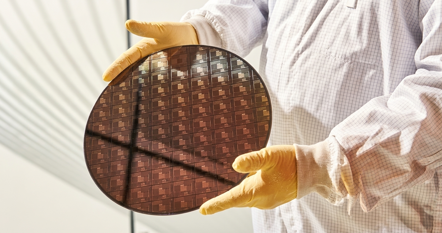
IBM's new "nanostack" 3D transistor architecture pushes chip manufacturing to 0.7 nanometers.
IBM just dropped a bombshell on the semiconductor world. The company has revealed a new chip manufacturing process operating at 0.7 nanometers — pushing well past what many industry leaders thought physically possible.
The secret sauce: a "nanostack" 3D transistor architecture that stacks components vertically rather than just shrinking them horizontally. IBM says this approach can sustain chip innovation for the next 10 years.
That timeline matters. The semiconductor industry has spent years fretting that the laws of physics would eventually slam the brakes on miniaturization. Transistors can only get so small before quantum effects wreak havoc. IBM's answer is to build up, not just down.
If the technology delivers on its promises, it could reshape the roadmap for processors powering everything from data centers to mobile devices for the foreseeable future.