ASML Eyes X-Ray Lithography as Chip Shrinking Nears Its Limit
Researchers explore metal-organic frameworks as photoresists to push silicon chips toward their absolute physical minimum.
The semiconductor industry is one technological leap away from the smallest silicon chips physically possible. And the path forward runs through some exotic chemistry.
ASML, the Dutch giant that dominates chipmaking equipment, is working to transition beyond its current extreme ultraviolet (EUV) lithography systems toward X-ray lithography. That jump demands entirely new materials.
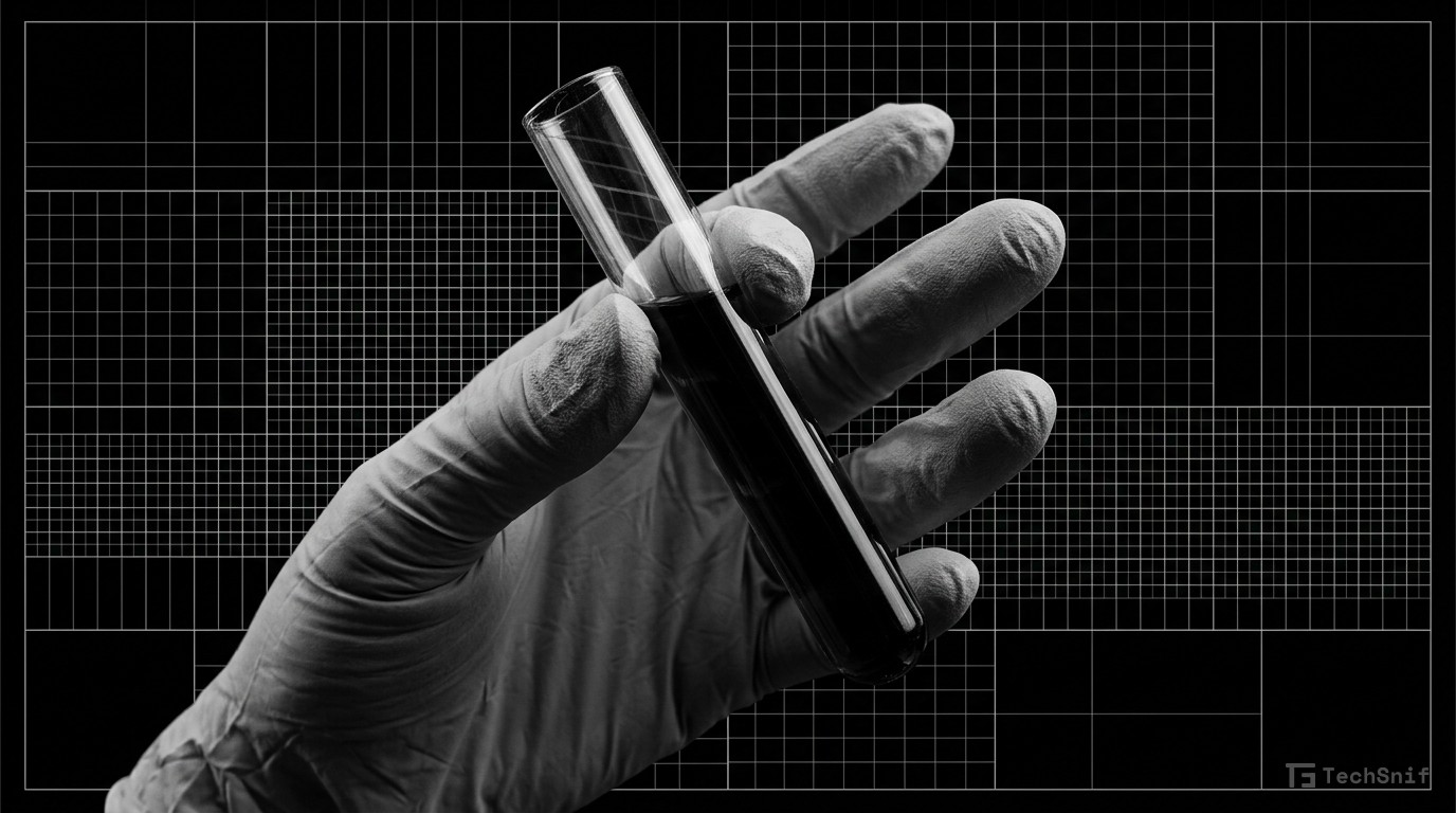
Researchers are investigating metal-organic frameworks — hybrid structures combining metal ions with organic molecules — as next-generation photoresists. These are the light-sensitive materials that define microscopic circuit patterns during silicon etching.
Current photoresists weren't designed for X-ray wavelengths. Metal-organic frameworks could solve that problem, enabling the precision needed at scales approaching atomic dimensions.
If it works, this is endgame territory for silicon. We're talking about chips fabricated near the fundamental physical limits of the material itself. No pressure.